Atomic precision,
built for volume.
SILICON operates 300mm wafer fabs for leading-edge logic, memory, and advanced-packaging customers. We carry the line from tape-out through high-volume manufacturing on a single qualified flow.
Engineering the line
between silicon and yield.
We design, qualify, and sustain the lithography, deposition, etch, and metrology stacks that bring next-generation processors from wafer to wafer with sub-nanometer repeatability.
Contact usSILICON develops and delivers fab-grade process flows for leading-edge logic, memory, and advanced packaging, qualified under continuous 24/7 operation.
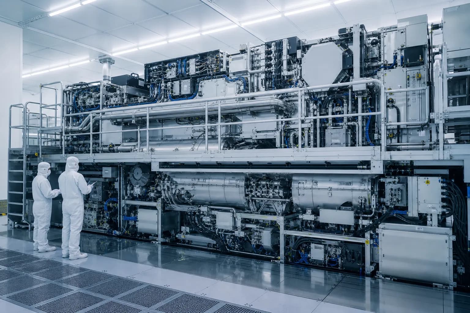

Every SILICON flow holds sub-nanometer overlay under continuous operation, lifting first-silicon yield curves and shortening ramp to volume. Process, yield, and sustaining engineers stay embedded through HVM exit.
Built for performance.
Qualified for volume.
Sub-5nm Capability
EUV-qualified line tuned for high-NA patterning and sub-0.5nm overlay across critical layers.
Yield-First Process
Mature recipes and SPC discipline lift first-silicon yield and compress the learning curve.
Copy-Exact Compliance
IATF, ISO 9001, and customer copy-exact qualifications maintained end-to-end on every line.
Tape-Out to HVM
One partner from NPI engineering lots through high-volume manufacturing and sustaining.

What process nodes does SILICON currently qualify?
Active lines span 5nm down to leading-edge 2nm logic, alongside DRAM and 3D NAND flows. High-NA EUV pilot capacity is online for sub-2nm research engagements.
How do you handle copy-exact transfers between fabs?
Tools are characterized against a reference chamber under customer recipe and passed through an SPC marathon before transfer. Match data is held to sub-3% variance on critical CD and overlay parameters.
Can engineering teams be embedded on the customer line?
Yes. Process, yield, and sustaining engineers can sit on-site through ramp, with handoff back to the customer team on a scheduled milestone or held indefinitely under a sustaining contract.
Do you support advanced packaging alongside front-end?
CoWoS, HBM stack qualification, and hybrid bonding run on the same qualified line as the front-end flow. Joint warpage and stack reliability are characterized against the packaging house spec.
What is the typical timeline from engagement to first wafer?
Plan of record inside week one, engineering lots within six to ten weeks depending on tool availability, pilot tape-out at the customer milestone. HVM exit follows the agreed yield ramp curve.
Which standards and certifications do you hold?
IATF 16949, ISO 9001, ISO 14001, ISO 14644-1 Class 1 cleanroom certification, and SEMI S2/S8 equipment safety compliance across every qualified line.
Send us the PDK.
We'll ramp the wafer.
Share your node, wafer volume, and target yield. A SILICON process integration lead responds within one business day with a qualification plan.