Equipment built for
atomic precision.
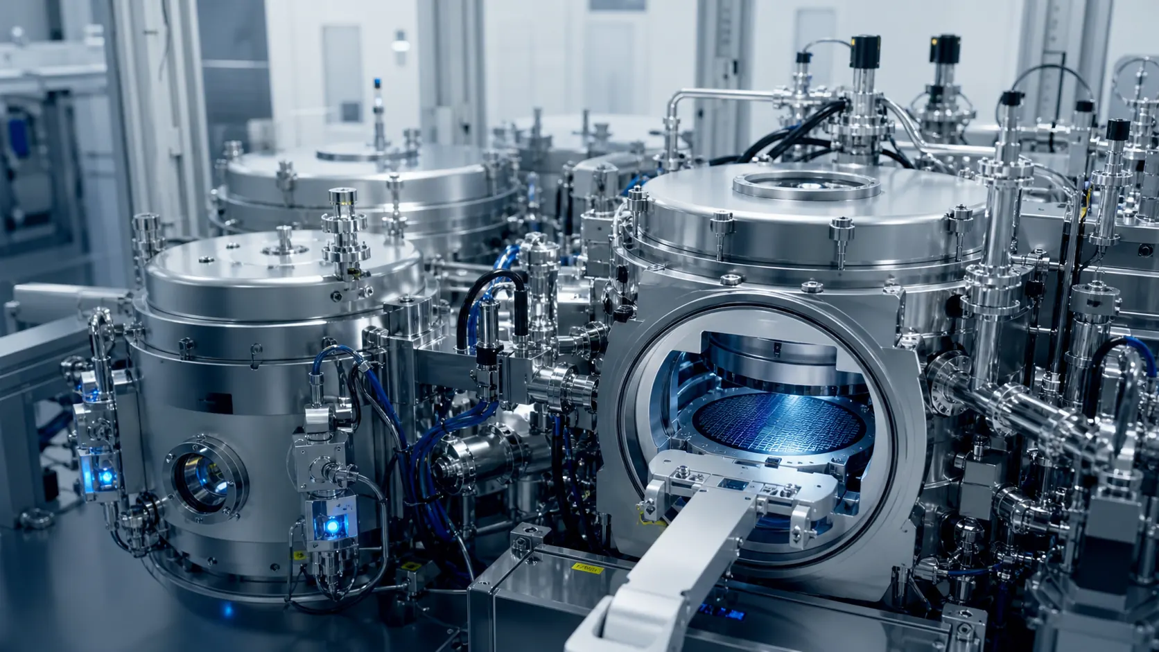
Front-end-of-line tools qualified for 300mm high-volume manufacturing, copy-exact across every SILICON line and tuned to hold sub-nanometer process windows under 24/7 load.
Four qualified clusters carry the critical layers, supported by wet clean, CMP, implant, anneal, PVD, and EPI modules that complete the front-end-of-line flow.
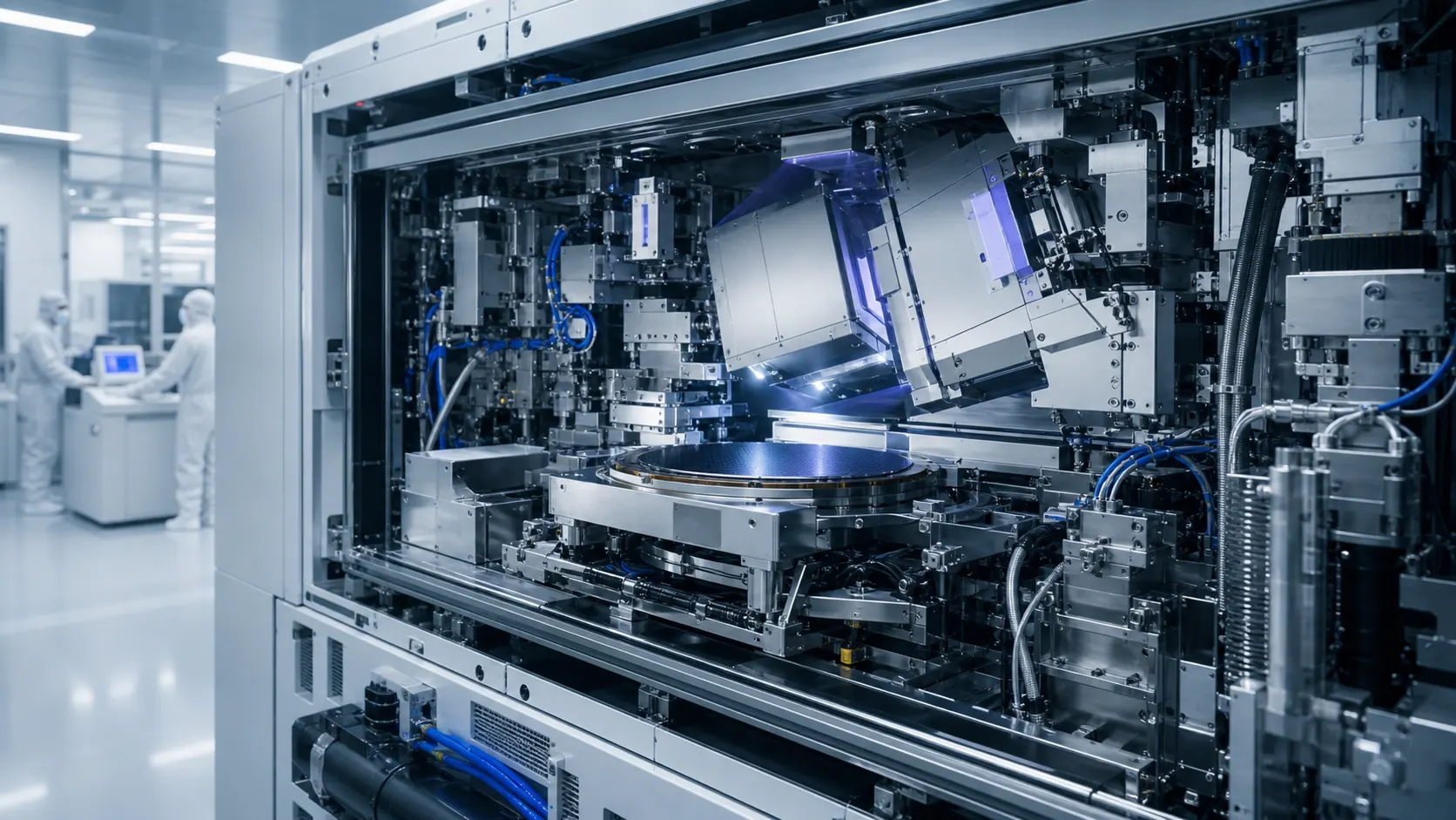
High-NA exposure scanners
Extreme ultraviolet patterning at 13.5nm, qualified for sub-5nm logic and DRAM front-end-of-line. Twin-stage wafer handling, in-vacuum reticle exchange, and pellicle-aware dose control hold critical dimension uniformity across the wafer.
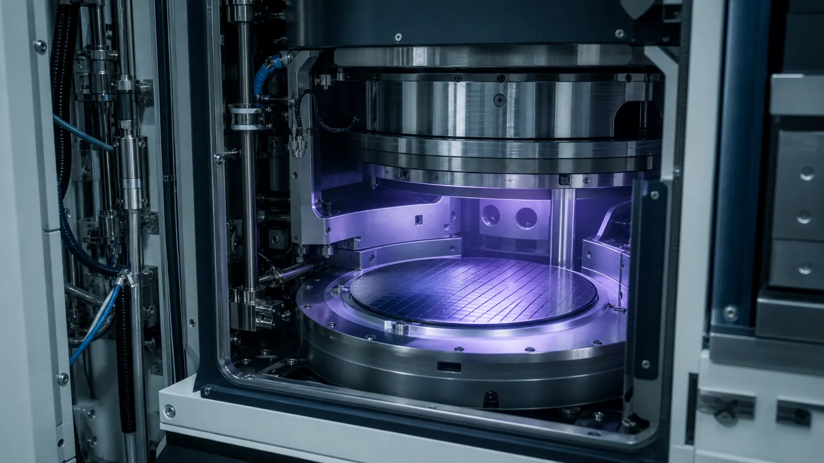
Monolayer-precise growth
Thermal and plasma-enhanced ALD systems for high-k dielectric, work-function metal, and barrier stacks. Self-limiting half-cycles deliver angstrom-level thickness control across 300mm wafers with sub-1% within-wafer non-uniformity.
Anisotropic dry processing
Inductively coupled and reactive ion etch chambers tuned for sub-3nm critical dimension control. In-situ optical emission spectroscopy and interferometry close the endpoint loop layer by layer, protecting underlying films from over-etch.
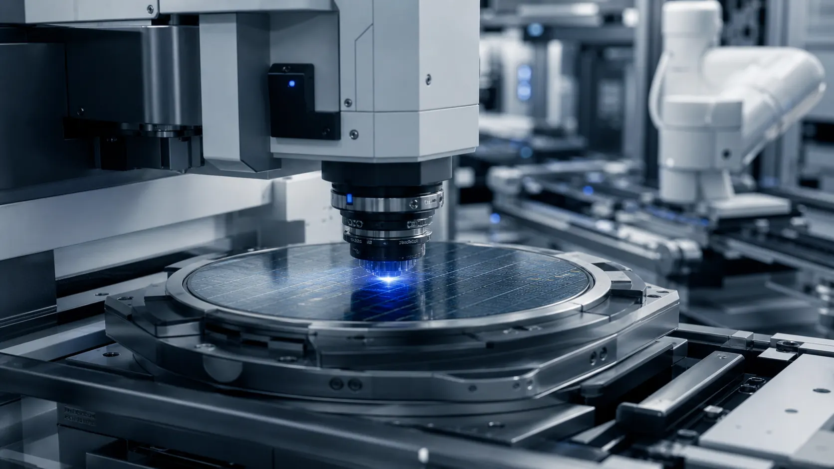
Inline measurement and defect control
CD-SEM, scatterometry, and broadband optical platforms feed the SPC stack at every critical layer. Sub-nanometer overlay sampling and full-wafer defectivity scans catch excursions inside the same lot, not after.
Six adjacent modules, one qualified recipe.
Every adjacent module sits inside the same SPC stack as the critical-layer clusters, so recipe portability and copy-exact qualification carry through the full flow.
Wet clean
Single-wafer SC1 / SC2 · ozonated DI
CMP
300mm planarization · 7-platen
Implant
Medium / high current · plasma doping
Anneal
Spike RTA · millisecond laser
PVD
Ionized barrier · seed-layer copper
EPI
Selective SiGe · group IV stacks
Tell us the node.
We'll match the tool.
Share your CD, overlay, and throughput targets. A SILICON equipment lead returns a qualification plan within one business day.