Sub-5nm silicon,
engineered at
atomic scale.
We design and operate the lithography, deposition, and metrology stacks that bring next-generation processors from wafer to wafer with sub-nanometer repeatability.
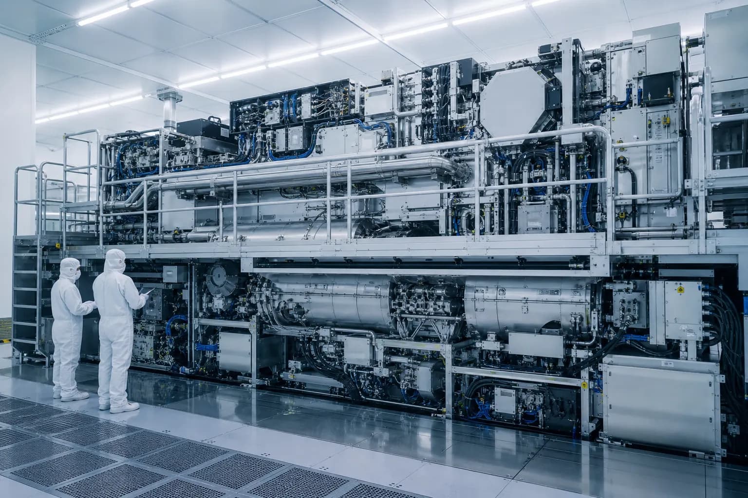
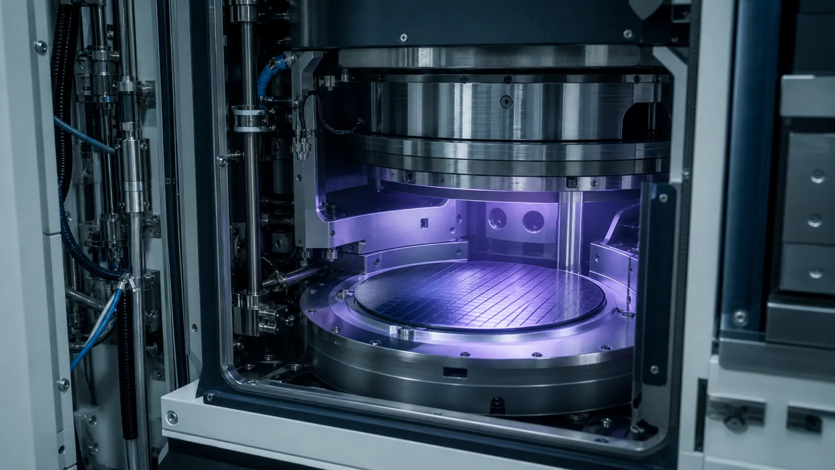
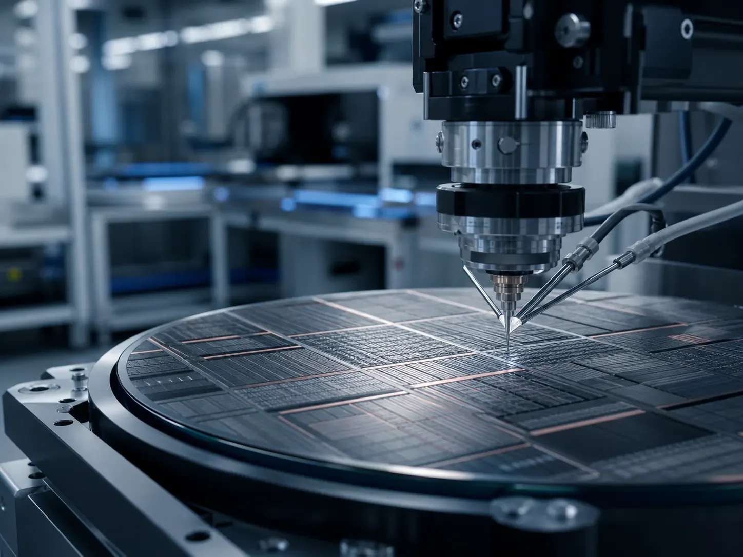
SILICON operates 300mm wafer fabs for leading-edge logic, memory, and advanced-packaging customers, from tape-out through high-volume manufacturing.

Every SILICON process is qualified to hold sub-nanometer overlay under continuous 24/7 operation, lifting first-silicon yield and shortening ramp to volume.
From bare silicon to packaged die, on a single qualified line.
Our tools hold tight to recipe under thermal, chemical, and particulate stress, qualified for high-volume logic, DRAM, NAND, and advanced packaging.
Process tools for leading-
edge node production.
EUV Lithography
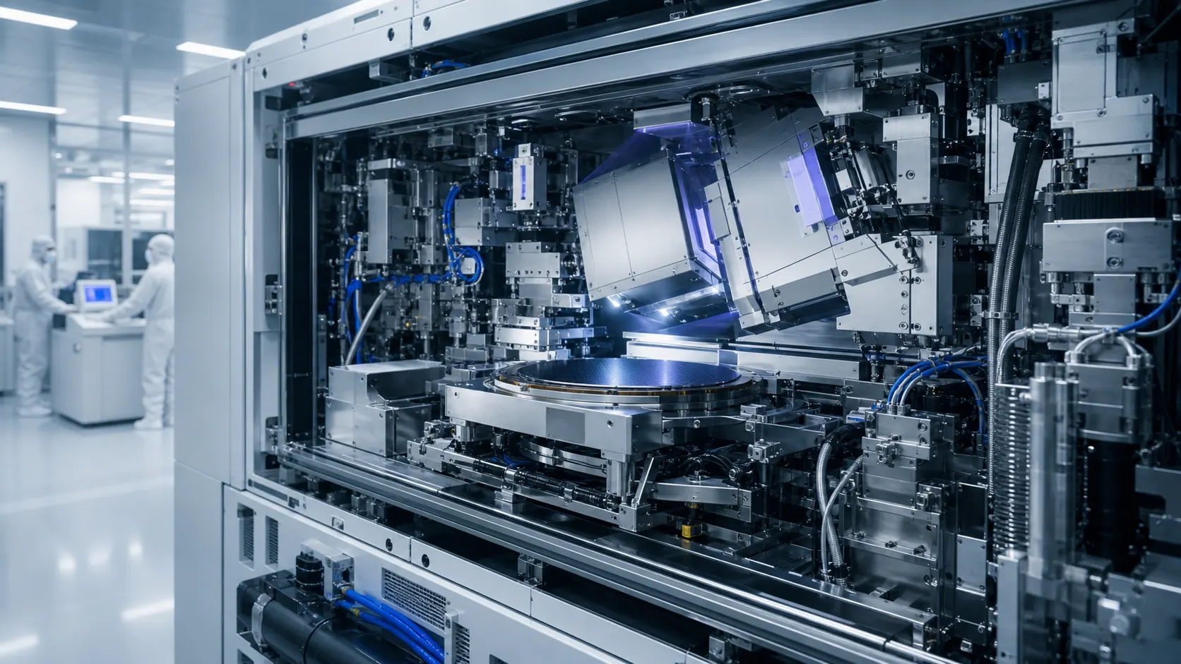
High-NA exposure scanners for sub-5nm patterning with sub-0.5nm overlay.
Atomic Layer Deposition
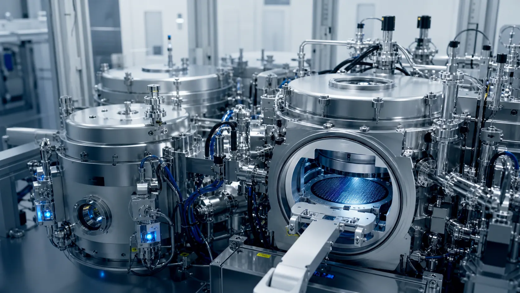
High-k dielectric and metal stacks deposited at angstrom-level repeatability.
Plasma Etch
Anisotropic dry etch with in-situ endpoint detection across the wafer.
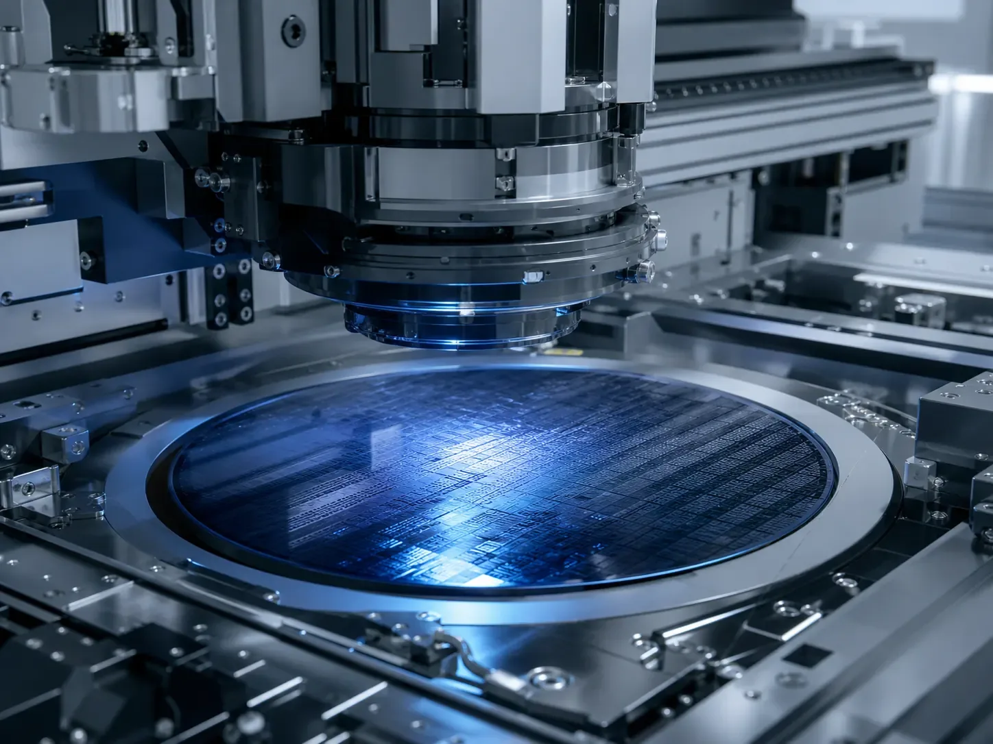
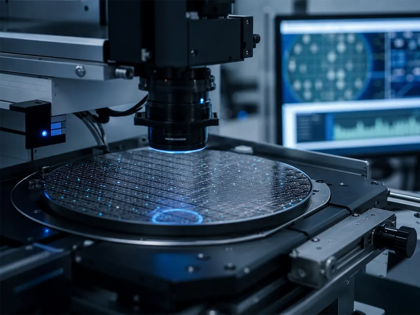
Metrology & Inspection
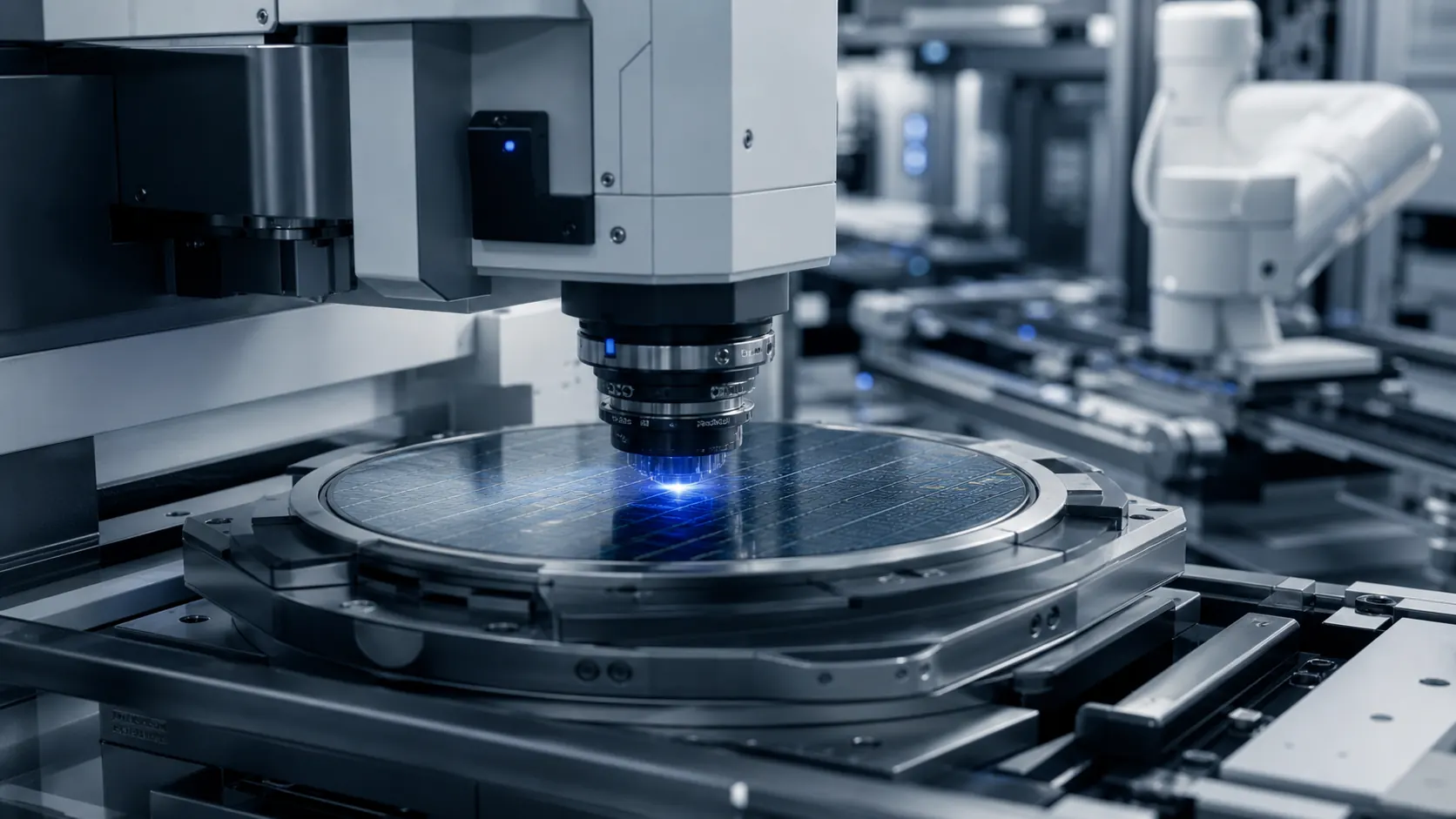
Inline defect inspection and overlay control at every critical layer.

Process Integration
We co-develop the front-end and back-end flow to hit your CD, overlay, and defect-density targets.
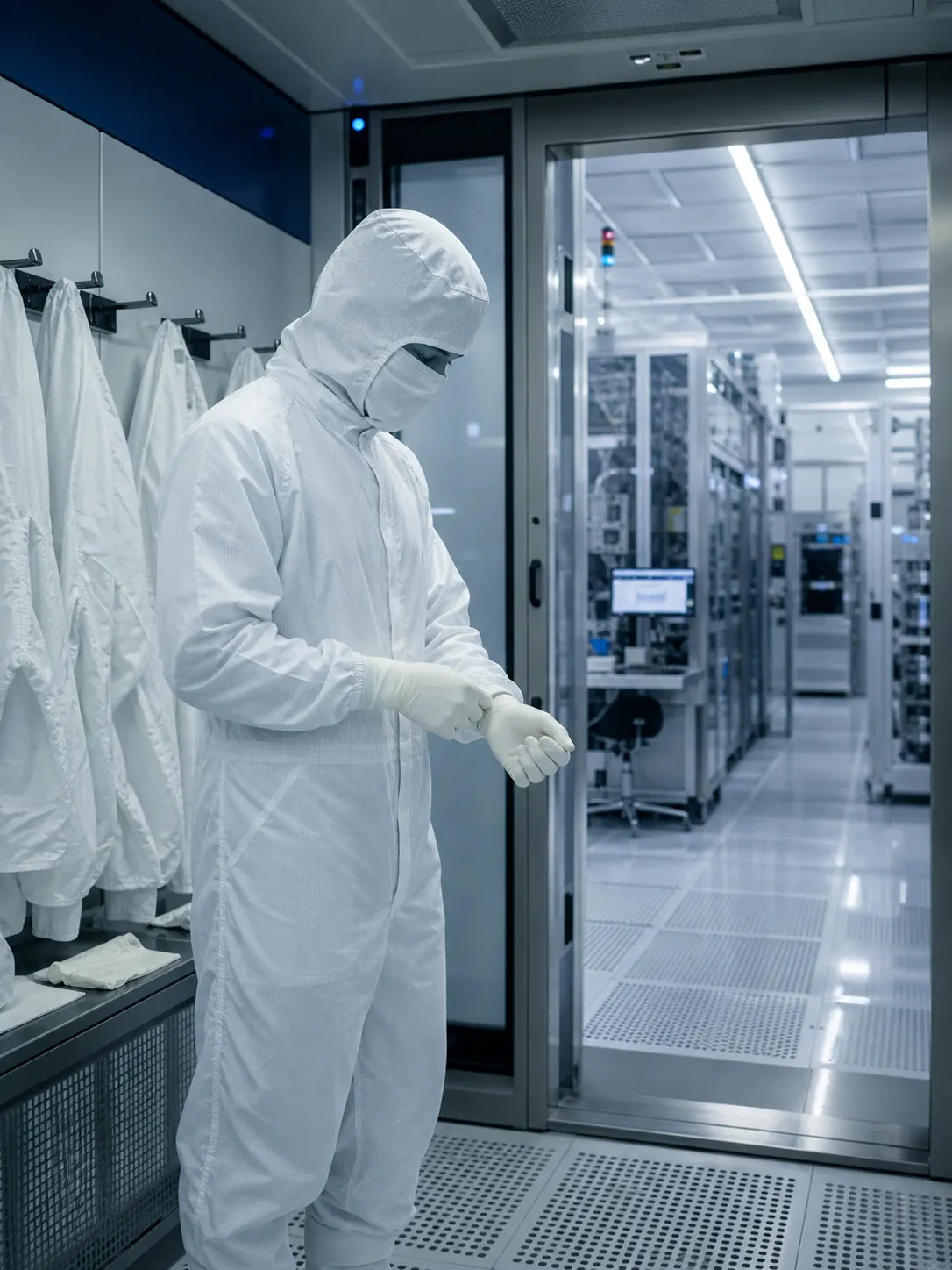
Tool Install & Qualification
Hookup, characterization, and copy-exact qualification to bring tools from FAT to first wafer.
Ramp to Volume
Dedicated engineers drive learning rate from engineering lots through high-volume manufacturing.
Sustaining & Uptime
Predictive maintenance and on-site response that protect tool availability and SPC stability.
Yield Engineering
Pareto-driven defect reduction and parametric tuning that pull learning curves forward by quarters, not months.
Metrology & Inspection
Inline CD-SEM, overlay, and optical control loops that hold sub-nanometer alignment across every critical layer.
Failure Analysis & Reliability
Cross-section, electrical, and accelerated-life analysis that closes the loop from field return to fab fix.
Advanced Packaging Support
Process integration and qualification for 2.5D, 3D, and hybrid-bonded stacks alongside the front-end flow.
Built for yield.
Qualified for volume.
Sub-5nm Capability
EUV-qualified line tuned for high-NA patterning and sub-0.5nm overlay.
High-Yield Process
Mature recipes and SPC discipline that lift first-silicon yield curves.
Copy-Exact Compliance
IATF, ISO, and customer copy-exact qualifications maintained end-to-end.
Tape-Out to HVM
One partner from NPI engineering lots through high-volume manufacturing.
Process notes for fab
and integration teams.
Send us the PDK.
We'll ramp the wafer.
Share your node, wafer volume, and target yield. A SILICON process integration lead responds within one business day with a qualification plan.