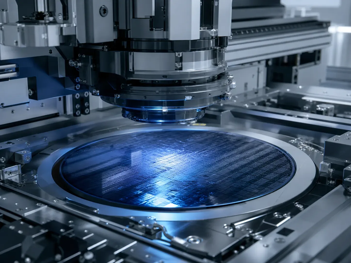
The stack changes on both sides
Backside power delivery is usually discussed as a routing improvement, but the manufacturing impact reaches into wafer thinning, via formation, bonding, and thermal control.
The metallization stack has to support lower IR drop while preserving the reliability margin already promised by the front-side flow.
Thermal and mechanical budgets converge
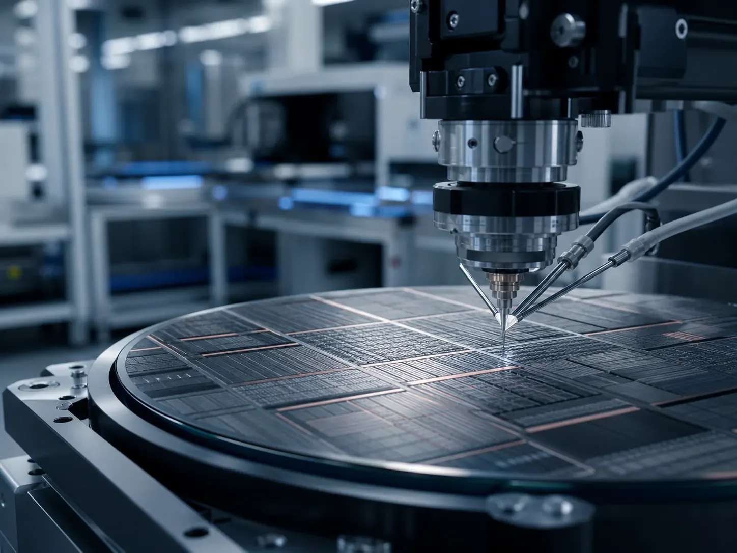
Wafer thinning and backside processing add stress states that can show up later as overlay drift, warpage, or reliability loss. These are integration problems, not isolated module issues.
SILICON qualifies backside modules against the same SPC stream used for the front-end route so excursions can be traced across the full stack.
Reliability starts during integration
The line needs early reliability evidence, not just end-of-flow validation. HTOL, HAST, and physical failure analysis should inform recipe decisions before the stack is frozen.
That is why backside power programs benefit from shared ownership between integration, metrology, packaging, and sustaining teams.